Vector Engine Type20 micro-architecture overview
Nov 1, 2020, Takuma SAITO (Processor Architecture Engineer), Satoru NAGASE (Processor Architecture Manager), AI Platform Division, NEC Corporation
Vector Engine, which is the heart of SX-Aurora TSUBASA, has been updated to 2nd generation (VE20). This document give an explanation on the overview of VE20 micro-architecture.
Vector Architecture
The vector is suited for large data processing
- High efficiency: a vector instruction can control 3kB data processing
- High usability: vector operation is easily enabled by auto vectorization compiler
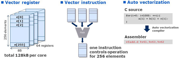
Vector Engine is particularly suitable for workloads processing a large amount of data, which can provide users with high efficiency and high usability. Vector architecture features large capacity of vector registers. Vector Engine has 64 set of vector registers and each register can accommodate 256 elements of 8Byte data (2kByte in total). And various vector instructions can process 256 elements of data all at once. NEC's dedicated vector compiler can automatically find where vectorization is applicable in your source code and output optimal assembly code. As special programing skill to do vectorization is not required, users can easily enjoy the benefit of powerful vector computing.
Data Size Comparison of SIMD and Vector
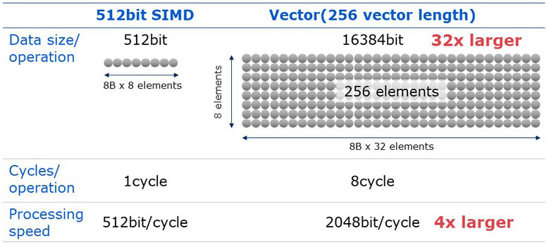
This slide shows schematic comparison between SIMD generally utilized in CPU (such as Intel x86 or Fujitsu A64fx) and Vector architecture utilized in Vector engine.
Typical 512bit SIMD deals with 8 elements of double precision data in one cycle. On the other hand, Vector engine can deal with the maximum of 256 elements (correspond to 16384bit SIMD) and operates 32 elements in one cycle which is 4times faster than 512bit SIMD.
As explained above, Vector processor can take care of a large amount of data by just one vector instruction. That is why Vector processor can realize high power-efficiency.
|
 |
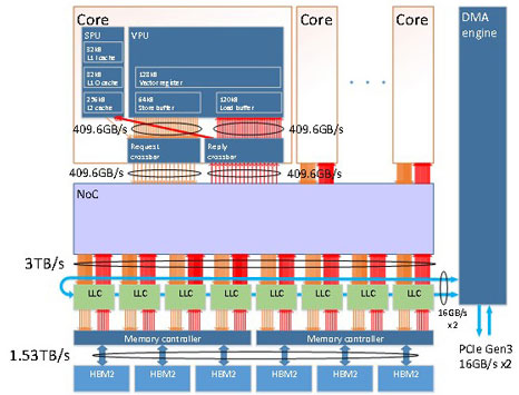
The image on the right shows the layout of Vector Engine Type 20 processor. VE20 processor is composed of 10 Vector cores (while previous VE10 has 8 Vector cores), LLC, HBM2 I/F (HBM2 memory controller), 6 HBM memories, DMA Engine and PCIe Interface.
Powerful Vector core works at the clock of 1.6GHz and can deliver as much as 307GF on Double precision and 614GF on Single precision. Total of 10 vector core, VE20's theoretical performance comes to 3.07TF on DP and 6.14TF on SP.
VE20 processor also includes 16MB of LLC (Last Level cache) which is divided into half and put at the both side of 10 cores. 10 vector cores and LLCs are connected with high bandwidth by multiple layer of 2-dimensional mesh networks called NOC (Network on Chip).
This high bandwidth NOC enable LLC to feed sufficient data to 10 vector cores. The detail structure of NOC is elaborated in later slide.
LLC is divided into multiple banks and each LLC bank has a connection to HBM2 memory controller. Total of 6 HBM2 controllers are placed near 6 HBM2s to control HBM2 memories respectively. HMB2 memory used for VE20 is newly enhanced, so total memory bandwidth increase up to 1.53TB/s which is 25% higher than 1.22TB/s of VE10. Following the previous VE10,VE20 is one of processors which have the world's highest level of memory bandwidth. This HBM2 controller is custom-made to deliver high memory load/store performance for various HPC and ML workloads.
One of notable features of VE20 is that it achieve the high B/F ratio (Byte per Flops ratio) of 0.5 which keeps higher ratio than other processors. It will contribute to deliver high effective performance in real HPC and ML applications. In addition, PCIe controller is located at the bottom of the ASIC die and has PCIe gen3 x16 interface to outside. Also DMA engine is located at the opposite side. It deals with data transfer between HBM2 memory and x86 host memory via PCIe interface.
After this slide, prime components of this processor are explained in detail.

Vector Core
- Vector Processing Unit (VPU)
- Powerful computing capability
- 307.2 GFLOPS DP/614.4 GFLOPS SP performance
- High Bandwith Memory Access
- 409.6 GB/S Load and Store
- Scalar Processing Unit (SPU)
- Provides the basic functionality as a processor
- Fetch, decode, branch, add, exception handling, etc. …
- Controls the status of the complete core
- Address translation and data forwarding crossbar
- To support continuous vector memory access
- 16 elements/cycle vector address generation and translation, 17 requests/cycle issuing
- 409.6 GB/sec load and 409.6 GB/sec store data forwarding
This slide shows an overview of vector core. The vector core consists of four major parts.
Vector Processing Unit (VPU)
VPU is the most characteristic unit of the Vector core. VPU has 128KB of Vector registers and provides powerful computing capability. Besides, VPU has a very powerful memory access capability and its theoretical memory bandwidth per core exceeds 400GB/s for load and store each.
Scalar Processing Unit (SPU)
SPU provides basic processor functions such as instruction fetch, decode, branch, and exception handling etc. It also plays a central role in processing and controls all other parts in vector core including VPU.
Address generation and translation / Data forwarding crossbar
Address generation and translation and Request crossbar make memory load/store packets and forward them to the right port of memory network. On the other hand, Reply crossbar forwards reply packets from memory network to 32 VPPs. These blocks are designed to support the continuous operation for VPU. In the vector processing, the pre-load feature is very important to hide the latency of memory load and avoid a lack of necessary data to Vector pipelines. When Address generation and translation block receives vector load instructions from SPU in advance, it can performs address translation for multiple vector elements having separate memory addresses all at once. And then it can make and issue up to 17 memory packets simultaneously. The Data forwarding crossbar can transfer memory load/store packets at the theoretical rate of 409.6GB/s for both load and store. These blocks are designed so that they have the same bandwidth as VPU's processing rate.
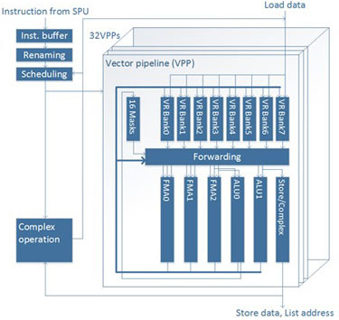
Vector Processing Unit
- Four pipelines, each 32-way parallel
- FMA0: FP fused multiply-add, integer multiply
- FMA1: FP fused multiply-add, integer multiply
- ALU0/FMA2: Integer add, multiply, mask, FP FMA
⇒ FMA0, FMA1, ALU0/FMA2: Total 96FMAs - ALU1/Store: Integer add, store, complex operation
- Doubled SP performance by 32bit x 2 packed vector data support
- Vector register (VR) renaming with 256 physical VRs
- 64 architectural VRs are renamed
- Enhanced preload capability
- Avoidance of WAR and WAW dependencies
- OoO scheduling
- Dedicated complex operation pipeline to prevent pipeline stall
- Vector sum, divide, mask population count, etc.
The right diagram illustrates the structure of Vector processing unit (VPU). VPU consists of 32 Vector pipelines called VPP and their control blocks such as Instruction buffer and renaming and scheduling blocks.
These control brocks decode the instruction from SPU and do renaming of Vector registers and scheduling and then finally give instruction to 32 VPPs at the same time.
VPP structure is very simple. The main components are the six execution pipelines and the transfer block among them. The six execution pipeline is as follows.
- 3 FMA pipelines (FMA0, FMA1, FMA2)
- 2 ALU pipelines (ALU0, ALU1)
- Store/Complex operation pipeline
"FMA2 and ALU0" and "ALU1 and store" share the read port, so the effective number of pipeline is four.
VPU design aims at two points. The first is to provide powerful computing capability.
To achieve that end, three floating point pipelines that support Fused multiply-add (FMA) are implemented. In total of 32 VPPs , it is possible for VPU to perform 96 FMA operations per cycle. It also supports the packed data type for vector operation which can doubles arithmetic performance for single precision compared to double precision.
Another goal is to maintain continuous operation of VPP. For that purpose, the register renaming function for vector register is introduced. VPU has 256 physical vector registers, and 64 architectural vector registers can be renamed to 256 physical vector registers. This contributes to improve the preload capability and avoid unnecessary WAR and WAW dependencies. Also VPU includes Out-of-Order Scheduling feature and offload s complex operations to dedicated complex operation pipeline outside VPP. This is aimed to prevent pipeline stall caused by the long latency of complex operations such as vector sum, divide etc.
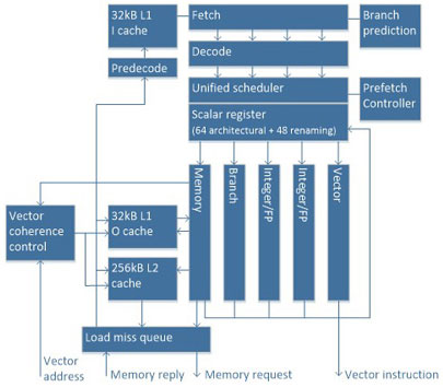
Scalar Processing Unit
- General enhancements
- 4 instructions/cycle fetch and decode
- Sophisticated branch prediction
- OoO scheduling
- 8-level speculative execution
- Four scalar instruction pipes
- Two 32 kB L1 caches + unified 256 kB L2 cache
- Hardware prefetching
- Support for continuous vector operation
- Dedicated vector instruction pipe
- 16 elements/cycle coherency control for vector store
SPU block diagram is shown on the right. The components of SPU are as follows.
- Fetch
- Decode
- Scheduler
- 5 pipelines
- 32KB L1 cache x2
- Instruction cache
- Operand cache
- 256KB L2 unified cache
SPU provides basic processor functions such as instruction fetch, decode, branch, and exception handling. It also controls other parts in the core such as managing the state of VPU.
The performance of Vector engine is largely provided by VPU, but the performance of SPU is also important. It is because SPU needs to process sequential part which cannot be vectorized, and also it needs to calculate the base address for vector memory access and dispatch sufficient vector instructions to VPU to fill a Vector pipelines.
SPU can fetch, decode and execute 4 instructions in parallel per each cycle. Many extensions are implemented such as advanced branch prediction and intelligent hardware prefetch to L2 cache.
In addition, the following enhancements are made to support efficient vector processing.
- Implement the dedicated vector pipeline to issue vector instruction to VPU.
- Vector cache coherent control block to support fast vector memory access.
Memory Subsystem
- High Bandwidth
- 409.6 GB/S x2 core bandwidth
- Over 3 TB/s LLC bandwidth
- 1.53 TB/s memory bandwidth
- Caches
- Scalar L1/L2 caches on each core
- 16 MB shared LLC
- Two memory networks
- 2D mesh NoC for core memory access
- Ring bus for DMA and PCIe traffic
- DMA engine
- Used by both vector cores and x86 node
- Can access VE memory, VE registers, and x86 memory
This slide describes the memory subsystem of Vector Engine. The strength of Vector engine is its memory bandwidth, so memory subsystem is designed to provide sufficient bandwidth from Vector core to memory.
Regarding cache hierarchy, three level of caches are implemented in Vector engine. L1 and L2 caches are located in SPU, which are private caches for instruction and scalar data. Last Level Cache (LLC) is the shared cache that is shared with all 10 Vector cores.
Regarding memory network, two kind of networks are implemented in Vector engine. The first one is NoC.
Each vector core is connected to NoC with the bandwidth of 409.6GB/s for load and store each. Also 8 distributed LLCs are connected to NoC and the total LLC bandwidth reaches 3TB/s. LLCs connected to six HBM2 memories via the Memory controller and the total memory bandwidth of HBM2 is 1.53TB/s (256GB/s x 6pcs).
The other is the ring bus. The bi-directional ring bus is implemented to connect all LLCs and DMA engine. The ring bus has the bandwidth of 16GB/s x2 (bi-direction) and is mainly used for PCIe and DMA traffic. DMA engine is virtualized and can be used from both vector cores and x86 simultaneously. In addition, DMA engine can access all memory address space such as x86 memory, VE memory and VE registers mapped to PCIe address space. As Vector engine has memory protection function, DMA engine can be used safely from user process.
Network on Chip (NoC)
- 2D mesh network
- Maximize bandwidth with minimal wiring
- Minimizing data transfer distance
- 16 layered mesh
- Deadlock avoidance
- Dimension-ordered Routing
- Virtual channels for request and reply
- Adaptive flow control
- Age based QoS control
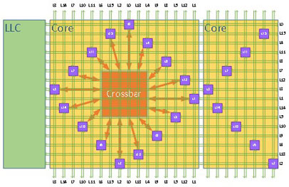
This diagram shows the physical image of Network on Chip (NoC) implemented in Vector engine. The 2D-mesh topology is introduced for NoC because the bandwidth can be maximized with limited wiring resource in the die and also the data transfer distance can be minimized. NoC is physically composed of 16 layer of 2D-mesh networks as shown the diagram. This makes it possible to transfer numerous data in parallel between all vector cores and LLCs.
The yellow box is a vector core and green box is LLC. Although not shown in the figure, another cores exist on top and bottom side.
The purple box is the Embedded router which is placed at the cross point of each layer and connects Vector cores and LLCs. The green wire indicates network wires connecting 2 routers and LLCs. The 16 layer of routers are aligned in a diamond shape in order to make use of limited wire resource effectively and to minimize the distance between the crossbar in vector core and the routers. These connecting wires are realized by using the upper metal layer in the die so that data can be transferred over long distance with low latency.
General functions such as dead-lock avoidance function and adaptive flow control and QoS control function based on age are implemented.

Last Level Cache (LLC)
- Memory side cache
- Avoiding massive snoop traffic
- Increasing efficiency of indirect memory access
- 16 MB, write back
- Inclusive of L1 and L2
- High Bandwidth design
- 128 banks, in total more than 3 TB/S bandwidth
- Auto data scrubbing
- Assignable data buffer feature
- Priority of data can be controlled by a flag for vector memory access instructions
This slide describes Last Level Cache (LLC). LLC is memory-side cache which is aimed to avoid massive snoop traffics and increase the efficiency of indirect direct memory access. LLC is inclusive of L1 and L2 caches and the total capacity of LLC is 16MB. To achieve as much as 3TB/s of bandwidth, LLC is divided into 128 banks (8 groups x 16 banks). LLC supports automatic data scrubbing function to prevent 1bit errors from accumulating and developing into multi-bit errors. And the assignable data buffer feature is implemented. By using this feature, user can control the replacement priority among caching data via the indication flag for vector memory access instruction.
- Intel and Xeon are trademarks of Intel Corporation in the U.S. and/or other countries.
- NVIDIA and Tesla are trademarks and/or registered trademarks of NVIDIA Corporation in the U.S. and other countries.
- Linux is a trademark or a registered trademark of Linus Torvalds in the U.S. and other countries.
- Proper nouns such as product names are registered trademarks or trademarks of individual manufacturers.